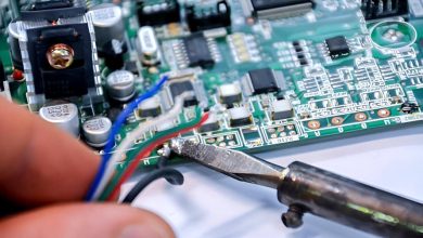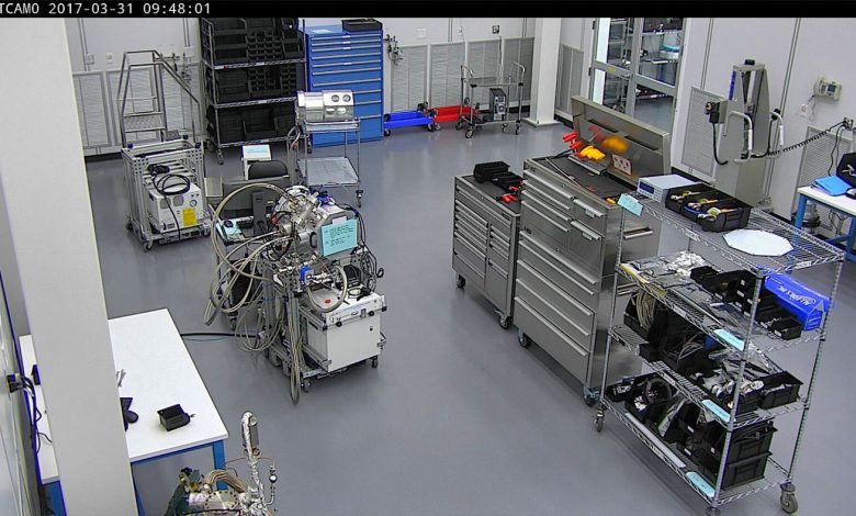
The race to build faster artificial intelligence processors is increasingly being won or lost not in transistor design but in packaging, the stage where silicon dies are stacked, linked and sealed into a finished chip. Modern AI accelerators combine logic, memory and interconnects from several separate pieces of silicon, joined with microscopic precision so they behave as one device. High-bandwidth memory stacks sit millimetres from the processor core, connected by thousands of tiny pathways that older packaging methods simply cannot provide. Foundries have responded by expanding packaging capacity as aggressively as they once expanded wafer production, and governments now treat advanced packaging plants as strategic assets worth subsidising. For chip designers, the change means performance gains increasingly come from architecture and assembly rather than from shrinking transistors alone, a profound shift in how the industry plans its roadmaps. The change is visible in hiring patterns, factory investment and government trade policy alike.
What the Evidence Shows
Packaging bottlenecks have already reshaped product launches, with several major accelerators delayed not by silicon shortages but by a lack of specialised substrate and interposer capacity. Engineers describe a craft that blends materials science, thermal management and mechanical engineering: stacked dies expand at different rates as they heat, and a package that warps by a fraction of a millimetre can fail. New approaches place chiplets on silicon bridges, embed connections inside the package itself and test each component before assembly so one faulty die does not ruin an entire module. The economics are shifting too, as packaging grows from a small share of a chip’s cost to a substantial fraction of its value. Analysts say the firms mastering this unglamorous stage now hold unusual power over the whole AI supply chain, and investment is following that reality. Major capacity announcements now arrive almost monthly across three continents. Reporting and analysis from sources such as MIT Technology Review track the same developments, and specialists following advanced packaging techniques for AI chips say the direction is now consistent across independent lines of evidence.
The Wider Context
The wider context is an industry learning to ship capability and restraint together. Products built around advanced packaging techniques for AI chips now launch with safety evaluations, usage data and rollback plans as standard, because enterprise buyers and regulators ask for them in the first meeting. Companies that treated those questions as friction are discovering they have become the purchase criteria.
What Happens Next
What happens next for advanced packaging techniques for AI chips depends less on another breakthrough than on the unglamorous work of reliability, pricing and support. The buyers evaluating it now are not enthusiasts; they are operators with budgets and auditors, and their checklists will decide the timeline. On the evidence of the current pilots, the technology has earned the right to be judged by them. You can follow related developments in our coverage of technology.
There is a practical lesson in all of this for readers deciding what to do today. Start with the verified facts, be wary of anyone promising certainty, and prefer reversible steps while the evidence is still developing. Circumstances differ by country, income and personal situation, so general guidance should always be weighed against your own context before you act on it in any significant or lasting way.